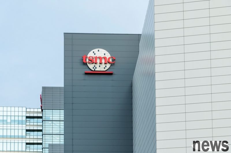
As the competition for AI chips becomes increasingly fierce, in order to maintain its leading competitiveness, the leading company NVIDIA (Nvidia) has reportedly obtained exclusive access to TSMC’s upcoming A16 semiconductor process capacity. This exclusive cooperation not only ensures NVIDIA's leading position in future chip technology, but also highlights that advanced packaging can become one of the bottlenecks in the AI chip supply chain amid tight advanced packaging production capacity.
Foreign media reported that NVIDIA and TSMC are currently conducting joint testing on the A16 process. The A16 process represents the next generation of chip technology, which is characterized by the use of nanosheet transistors and Super Power Rail technology. NVIDIA is expected to use the A16 node process to produce its next-generation Feynman GPU architecture, which is expected to be released in 2028.
It is worth noting that the A16 process technology puts forward higher requirements for the advanced packaging of the GPU, which requires more through-silicon via (TSV) channels to have better connection and heat dissipation control capabilities. In fact, advanced packaging technology, especially TSMC's CoWoS, has become a key bottleneck limiting the supply of AI chips, and NVIDIA has a great advantage in this battle. According to data, NVIDIA has ordered 70% of TSMC’s CoWoS-L annual production capacity in 2025.
Under this circumstance, the tight production capacity of TSMC CoWoS has also created market opportunities for outsourced packaging and testing service providers (OSATs) and equipment manufacturers. In order to deal with this bottleneck, TSMC is actively developing alternatives, including CoPoS, and planned wafer-level packaging, and adding new equipment and partners to meet the huge market demand.
In addition, HBM’s supply and advanced packaging also control the competitive landscape of AI chips. The current stack height of HBM3E is 12 layers. In the future, HBM4 is expected to reach 16-layer stacking, which will likely require the use of hybrid bonding technology, especially on HBM4E. In this case, the production bottleneck of advanced packaging has made HBM4 suppliers nervous.
In addition, facing supply chain constraints, large cloud service providers (Hyperscalers) and their chip startups are being affected by TSMC's CoWoS supply shortage. To reduce dependence on external suppliers, the industry is adopting several strategies including establishing alternative packaging lines and moving toward vertical integration. Among them, vertical integration means bringing more links from design to manufacturing stack under its own control to ensure the resilience of the supply chain.
Overall, NVIDIA has built towering barriers in the competition for next-generation AI chips by locking in TSMC’s cutting-edge A16 process and combining it with its huge reservations in CoWoS production capacity. Other participants in the industry must break the current supply chain bottleneck and compete for the future AI computing power market through innovative packaging technologies and implementation of vertical integration strategies.